- Home
-
SiC Crystal Growth Trends and Manufacturing Challenges for the Next Five Years
JAN. 5, 2026Silicon carbide (SiC) has rapidly moved from a niche semiconductor material to a strategic foundation for power electronics, especially in electric vehicles, renewable energy systems, and high-voltage industrial applications. As demand for higher efficiency, higher power density, and higher temperature tolerance continues to rise, SiC substrates are becoming indispensable. At the center of this shift lies one critical process: SiC crystal growth.
Over the next five years, improvements in crystal quality, wafer size, and manufacturing stability will largely determine how fast SiC can scale—and how competitive manufacturers can become.
Key Trends in SiC Crystal Growth Technology
One of the most visible trends is the transition toward larger-diameter wafers. The industry is steadily moving from 6-inch to 8-inch SiC substrates, driven by cost reduction and higher throughput requirements. However, scaling wafer size is not simply a matter of enlarging furnaces—it places much higher demands on temperature uniformity, thermal field control, and defect suppression during crystal growth.
Another important direction is the push for lower defect densities, particularly micropipes and basal plane dislocations. As SiC devices enter automotive and grid-level applications, tolerance for crystal defects continues to shrink. This drives tighter process control and more advanced monitoring throughout the growth cycle.
Manufacturing Challenges That Still Limit Scale-Up
Despite steady progress, SiC crystal growth remains one of the most technically demanding processes in semiconductor manufacturing. High growth temperatures, long cycle times, and narrow process windows make consistency difficult to maintain—especially at scale.
Two challenges stand out in real production environments:
1: Thermal field stability remains a constant concern. Small fluctuations in temperature gradients can directly affect crystal quality and defect formation. Maintaining long-term thermal consistency places high demands on furnace design, heating systems, and control algorithms.
2: Yield management becomes increasingly complex as wafer sizes grow. A single defect can impact a much larger usable area, amplifying yield losses and driving up costs if process control is insufficient.
The Role of Equipment Intelligence in the Next Five Years
Looking ahead, equipment intelligence will play a decisive role in overcoming these challenges. Crystal growth systems are evolving from static, recipe-driven tools into adaptive platforms capable of real-time monitoring and process adjustment.
Advanced sensors, data analytics, and closed-loop control systems allow manufacturers to better manage temperature fields, improve repeatability, and detect anomalies earlier in the growth cycle. Over time, this intelligence not only improves yield but also shortens learning curves when scaling to larger wafers or new crystal structures.
About ATW
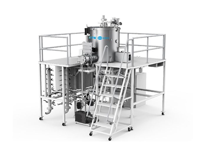
ATW is an advanced equipment manufacturer with deep expertise in crystal growth and high-temperature process control technologies. Leveraging experience from semiconductor and advanced materials manufacturing, ATW provides intelligent equipment solutions designed to support stable SiC crystal growth, improved thermal field uniformity, and scalable production.
As SiC manufacturing moves toward larger wafers and stricter quality requirements, ATW continues to work closely with customers to optimize process stability, improve yield, and prepare production lines for the next generation of wide-bandgap semiconductor technologies.
Contact ATW to explore how intelligent equipment can help you meet the challenges of SiC crystal growth over the next five years.


