

- Home
-
SemiconductorSemiconductor Products
Semiconductor products are electronic components made from materials like silicon that can control electrical currents. They form the basis of devices such as diodes, transistors, and solar cells. Leveraging core technologies like precision dispensing, IPC systems, ultrasonic bonding, and non-destructive pull tests, ATW focuses on the development of high-performance die bonders and aluminum wire bonders to provide highly efficient semiconductor packaging solutions for global customers.
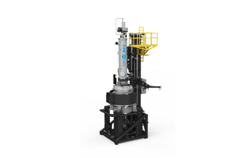
Crystal Growth
Crystal growth is the process of forming large, defect-free single crystals from raw materials, which serve as the foundation for semiconductor wafers. High-quality crystals, such as silicon ingots, are essential because even tiny defects can affect the performance of microchips. Controlled crystal growth ensures uniform electrical, optical, and mechanical properties, making it critical for reliable and efficient semiconductor devices. This step underpins the entire semiconductor fabrication chain, from integrated circuits to advanced electronic systems.
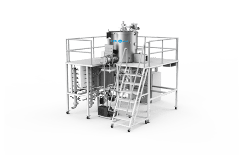
CMP
Chemical Mechanical Planarization (CMP) is a polishing process used to smooth and flatten wafer surfaces during semiconductor fabrication. It removes excess material and ensures a uniform, defect-free layer, which is vital for precise photolithography and multi-layer chip structures. By achieving an even surface, CMP improves device performance, reduces defects, and enables the scaling of advanced semiconductor technologies.
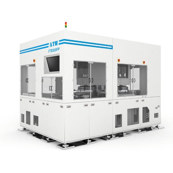
Assembly & Test
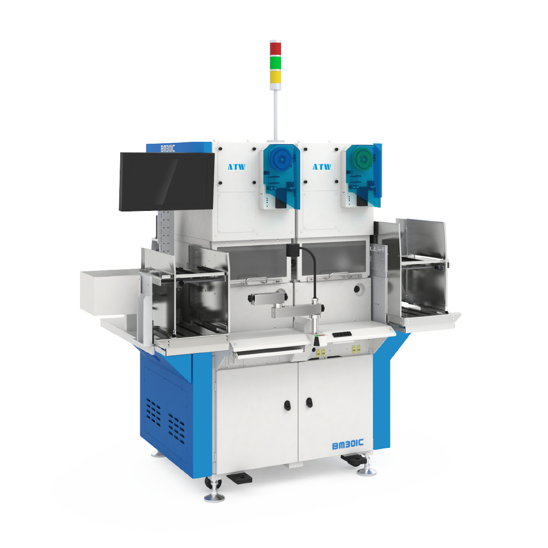
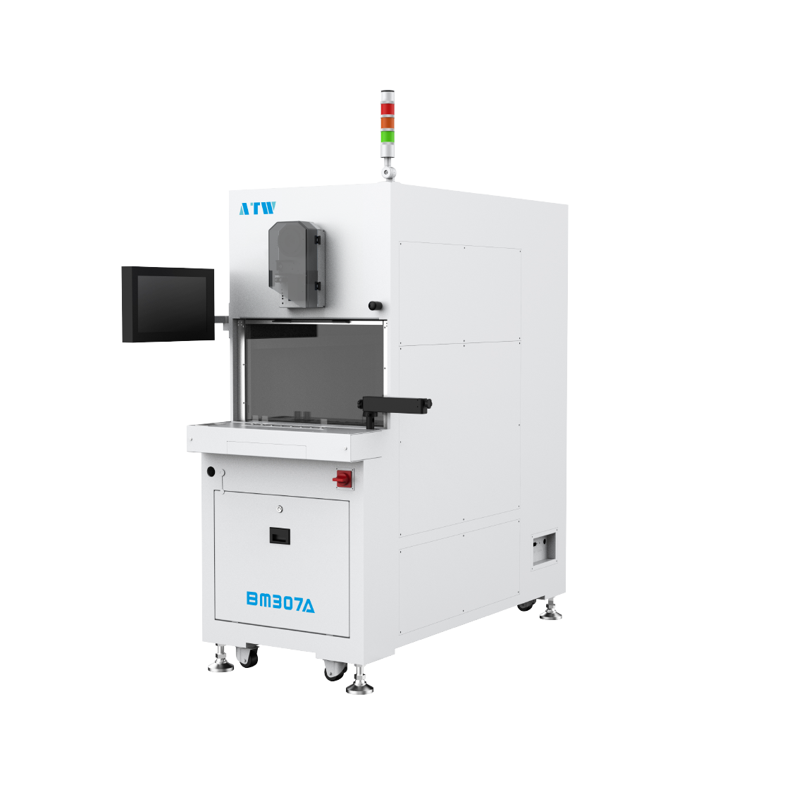
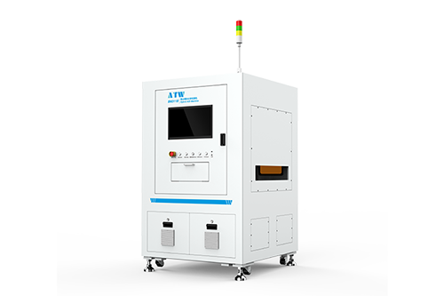
The use of advanced, specialized machinery—such as wire bonders, AOI systems, wafer cleaners, and dicing machines—is crucial for assembling and testing semiconductor products with precision and reliability. These tools ensure accurate interconnections, defect detection, contamination-free surfaces, and precise wafer cutting, all of which directly impact yield, performance, and long-term device reliability.
-
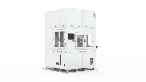
Automatic 12" Twin Spindle Dicing Saw LFD7100
-
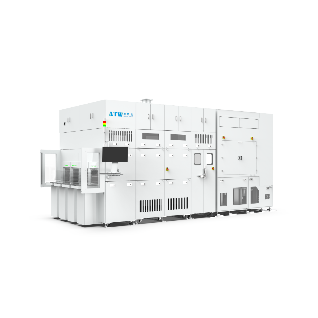
Automatic 8" Single Spindle Dicing Saw LAD5100
-
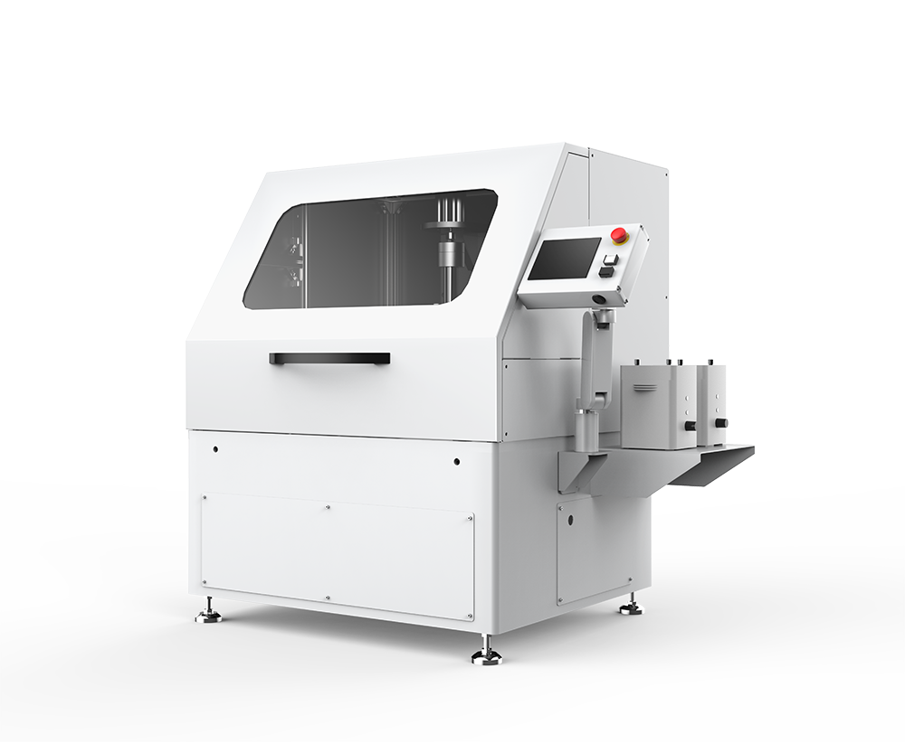
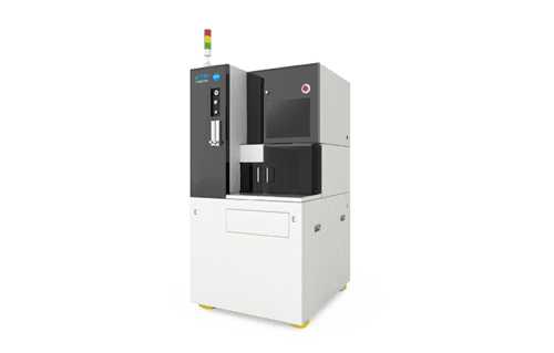
Wafer Cleaner LAC200
-
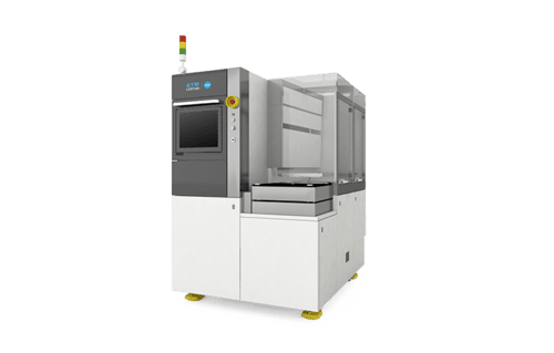
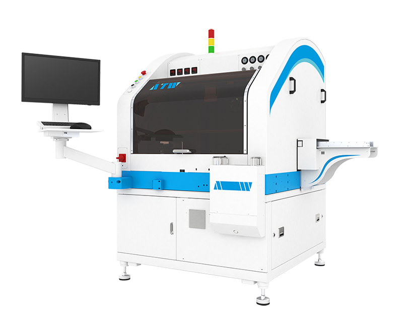
Automatic High speed Epoxy Die Bonder
-
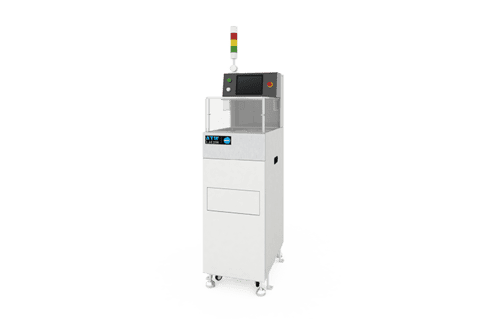
Soft Solder Die Bonder
-
Multifunction Die Bonder
-
Aluminum Wire Bonder
-
Hybrid Aluminum Wedge Bonder
-
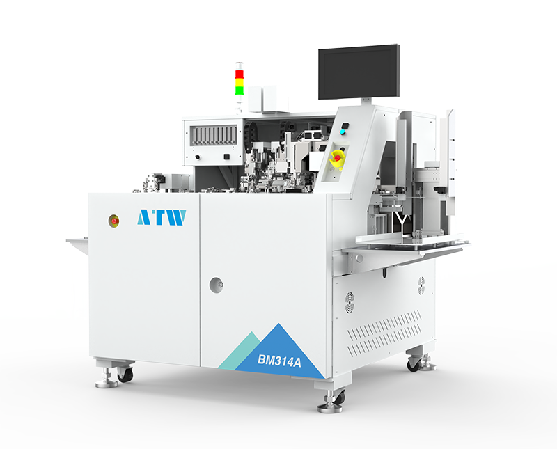
Hybrid AOI Machine BM311B
-
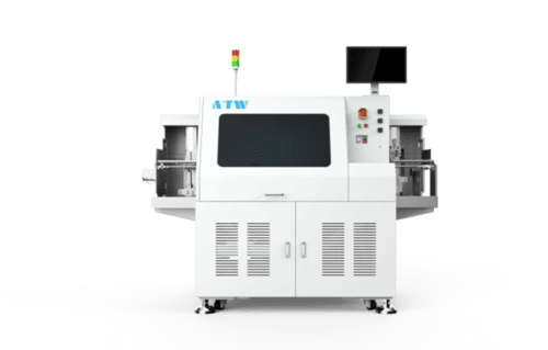
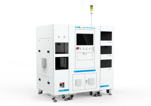
DB/WB AOI Machine BM310B
-