


Photovoltaic Products
Wafer Inspection System
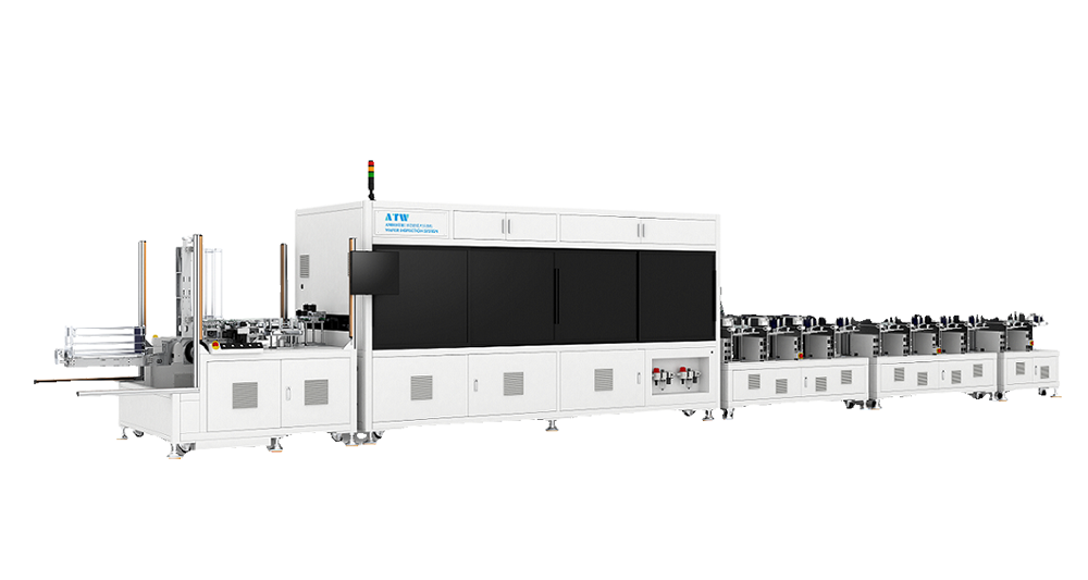
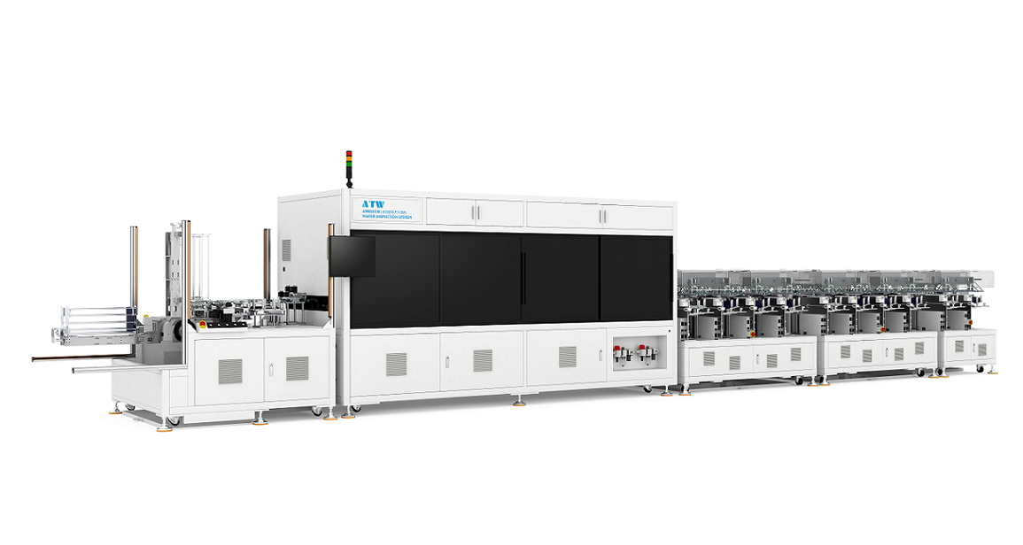
AM018T wafer inspection system is a fast, accurate and comprehensive solution allowing you to detect and sort wafers by size, thickness, stain, chipping, resistivity, micro crack, P/N type, hole, etc.
-
Suitable for
180-230mm wafer
The pioneer of wafer sorting system in domestic market
Leveraging the excellent inspection performance and reliable automation, the inspection system gained good reputation and became the first choice of global customers.
The High-speed Wafer Inspection System is specifically designed for the end-of-line quality inspection following slicing and cleaning processes in wafer manufacturing, and serves as the ultimate quality check before shipment of wafers.
Core function: Perform comprehensive inspection and grading of wafers, ensuring that only qualified wafers enter the cell manufacturing process, thereby achieving better quality at more competitive prices.
The data generated by the wafer inspection system can also be transmitted to the previous slicing process for process optimization and yield improvement.
Technological advantages:
a) Essential equipment for the mass production of high-efficiency solar cells, addressing the trend towards large-size (182-230mm full and half-cut) and thinner wafers (100-240μm);
b) AI-based inspection: The combination of traditional algorithms and deep learning enables it to identify complex defects such as micro-crack (length ≥ 0.5mm), saw mark (±3µm), and TTV (±2µm) more accurately and stably, with a detection rate exceeding 98%;
c) High stability and low breakage ratio: Leveraging Bernoulli-type non-destructive transfer technology, it keeps the breakage ratio at an extremely low level (e.g., < 0.1%) even running at a high speed, ensuring continuous production and stability.
-

 Smart system
 -

 Function design
 -

 AI intelligent inspection
 -

 Flexible extension