


How Is SiC Crystal Growth Evolving, and What Challenges Remain for Equipment Manufacturers?
DEC. 3, 2025
Silicon carbide (SiC) has quickly moved from a “cutting-edge material” to a core driver of modern power electronics. Whether in electric vehicles, renewable energy, industrial automation, or energy storage, the shift toward higher efficiency and higher power density is pushing SiC to the center of attention. Yet behind every high-performance SiC device is a long and technically demanding crystal growth process — one that continues to promote but still faces some unique challenges.
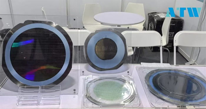
SiC wafer
How SiC Crystal Growth Is Evolving
One of the clearest trends in SiC crystal growth industry is the transition from 6-inch to 8-inch SiC wafers. The industry is eager for the higher throughput and lower cost per device that larger wafers can deliver. But growing bigger crystals is not simply a matter of scaling the equipment — it requires more refined temperature control, more stable pressure regulation, and a deeper understanding of the thermal field inside the furnace.This is why today’s SiC furnaces place such a strong emphasis on multi-zone temperature control, dynamic crucible movement, and precision pressure systems. ATW TECHNOLOGY’s latest SiC Crystal growth furnaces integrate these features to help customers maintain growth stability even during long cycles that may last more than 100 hours.

SiC Crystal Growth Furnace
Another noticeable shift is the push toward intelligent, automated growth. Because long-duration crystal growth processes amplify even minor fluctuations, manufacturers increasingly rely on automated control systems, real-time monitoring, and remote supervision to maintain consistency. Intelligent control software, AI-based detection, and centralized control and management are now becoming practical tools rather than future concepts.
Energy Consumption of Crystal Growth has also become an unavoidable topic. Crystal growth at extremely high temperatures consumes significant energy, so equipment that can maintain hot zone uniformity while reducing heat loss is highly valued. ATW TECHNOLOGY’s recent designs focus heavily on lowering energy consumption without sacrificing stability — a balance that many customers are actively pursuing.
The Challenges That Still Stand in the Way
Despite these advancements, SiC crystal growth is still one of the most demanding processes in semiconductor manufacturing.Defect control remains a key challenge. Micropipes, basal plane dislocations, and stacking faults are not easily eliminated, and each type of defect influences downstream device performance in its own way. Achieving low-defect crystals growth requires extremely consistent growth environments, something that tests the limits of thermal and pressure control systems.
Maintaining pressure stability at temperatures beyond 2,300°C is another major challenge. At these extremes, even the smallest mechanical deformation or thermal drift can impact crystal structure. For equipment manufacturers, this demands a supreme level of mechanical design capability, coupled with manufacturing expertise in precision feedback systems.
Scaling up to 8-inch wafers adds growing system’s further complications — such as increased stress in the hot zone, more complex thermal management, and higher risks of crystal phase transition. These engineering issues have become a shared focus across the industry.
And of course, the process is inherently long and energy-intensive. Reducing cycle time while protecting crystal quality is still a balancing act shared by all SiC manufacturers.
Beyond equipment, there is also a knowledge gap. SiC crystal growth isn’t just about hardware; it relies on accumulated experience. Many manufacturers of SiC crystal depend on deep engineering support and data-driven insights to fine-tune recipes, troubleshoot variation, and stabilize production.
How ATW TECHNOLOGY Contributes to the Field
At ATW TECHNOLOGY, we aim to support SiC manufacturers with a combination of high-precision furnace design, intelligent control systems, and cross-industry expertise built from our work in PV crystal growth, semiconductors, and lithium-ion manufacturing.Our SiC crystal growth furnaces are equipped with multi-zone temperature control, dynamic crucible management, precision pressure systems, and remote centralized control. These features help stabilize long-cycle growth and improve yield consistency. Meanwhile, our intelligent systems — including AI-based monitoring and integrated manufacturing platforms — help customers detect anomalies earlier, manage data more effectively, and gradually improve growth quality over time.
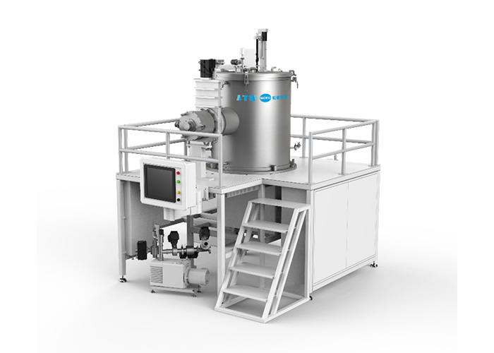
SiC Crystal Growth Furnace
Looking Ahead
SiC will continue to play a central role as industries move toward electrification and higher energy efficiency. The progress we see today is only the beginning. Larger wafers, smarter equipment, and greener manufacturing will define the next stage of development.While challenges in defect control, temperature uniformity, pressure stability and scale-up remain, the direction is clear: SiC production will become more automated, more intelligent, and more cost-efficient.
With its strong engineering foundation and commitment to intelligent manufacturing, ATW TECHNOLOGY is determined to help customers accelerate SiC adoption and build reliable, high-quality, large-scale crystal growth operations.